【專利核准公告】P92009A-以薄膜層進行銅導線晶片之銲線製程方法「WIRE-BONDING METHOD FOR CHIPS WITH COPPER INTERCONNECTS BY INTRODUCING A THIN LAYER」(已終止維護)

|
專利國別 |
美國 |
發表日期 |
2012-06-22 09:51:25 |
|
本校案號 |
P92009A |
||
|
專利名稱 |
以薄膜層進行銅導線晶片之銲線製程方法「WIRE-BONDING METHOD FOR CHIPS WITH COPPER INTERCONNECTS BY INTRODUCING A THIN LAYER」 |
||
|
發明人 |
鄭友仁、邱桑茂 |
||
|
所屬院 |
工學院 |
提案單位 |
機械工程學系暨研究所 |
|
類型 |
發明 |
專利權人 |
國立中正大學 |
|
申請號 |
10/855,161 |
申請日期 |
2004-05-26 |
|
公開號 |
US20050266672A1 |
公開日期 |
2005-12-01 |
|
證書號 |
US 6,962,864 B1 |
核准日期 |
2005-11-08 |
|
國際分類號 |
H01L-021/02(2006.01);H01L-021/44(2006.01) |
||
|
專利權期間 |
2004.05.26~2024.05.26 |
||
|
專利摘要 |
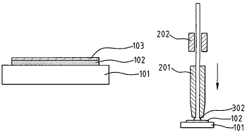
A wire-bonding method for chips with copper interconnects by introducing a thin layer is provided for solving the problem of oxidizing a copper bonding-pad during bonding processing in order not to deteriorate the bonding strength and yield rate thereof. The wire-bonding method of the present invention comprises: a step for providing a chip with a copper bonding-pad; another step for providing an aqueous solution to form a Cuprous oxide thin layer on the copper bonding-pad; and yet another step for setting a plurality of copper interconnects on the copper bonding-pad and providing an ultrasonic power for removing the Cuprous oxide layer to have the interconnects bonded on the copper bonding-pad. |
||
|
圖示 |
|||